Yes, China must develop its own modern advanced immersion lithography machine because the West has drawn up the hostile and unfair Wassenauer Agreement against China, the Agreement on Export Control of Conventional Arms and Dual-Use Goods and Technologies.
是啊,中国必须发展自己的现代先进的浸没式光刻机,因为西方对中国拟定了敌对和不公平的《瓦森纳协议》,即《常规武器和军民两用货物和技术出口管制协议》。
Chinese companies need to participate more in the semiconductor industry chain, which may not have much impact now, but its importance will be highlighted in the future. There is still a big gap between the Chinese semiconductor industry and its international counterparts, and overall, they are still trying to catch up.
中国企业需要更多地参与到半导体产业链中,这一点现在可能没有太大的影响,但未来的重要性将会凸显出来。中国半导体产业与国际同行之间仍有很大差距,总体而言,他们仍在努力追赶。
Some small specialized, refined, characteristic, innovative companies, although rarely appear in the spotlight, but they silently target market segments, and strive to polish some products, successfully gain a foothold in the global semiconductor industry chain, and stabilize this trillion-level market.
一些小的专业化、精细化、有特色、有创新的公司,虽然很少出现在聚光灯下,但他们默默地瞄准细分市场,努力打磨一些产品,成功地在全球半导体产业链中站稳脚跟,稳定了这个万亿级的市场。
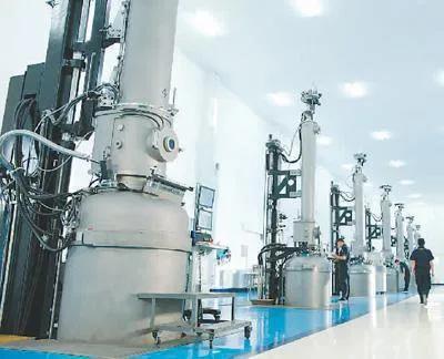
The above image shows an interior view of the Thinkon Semiconductor monocrystalline silicon rod workshop.
上图显示了Thinkon半导体单晶硅棒车间的内部视图。
Thinkon Semiconductor started producing monocrystalline silicon for etching because it was also quite profitable and had a lot in common with wafer production.
Thinkon半导体(Thinkon Semiconductor)开始生产用于蚀刻的单晶硅,因为利润也相当可观,而且与晶圆生产有很多共同点。
During wafer etching, silicon electrodes made of monocrystalline silicon are consumed at the same time as the wafer and need to be larger than the wafer size. For example, to process a 12-inch wafer, the size of the corresponding monocrystalline silicon material used for etching is usually at least 14 inches. In order to reduce costs, as the chip manufacturing process has advanced from 28 nm to 7 nm or even 5 nm, the mainstream wafer size used in advanced processes has increased from 8 inches to 12 inches or larger. This also means that the size of the monocrystalline silicon used for etching must be increased accordingly.
在晶圆刻蚀过程中,由单晶硅制成的硅电极与晶圆同时消耗,需要比晶圆尺寸更大。例如,要加工12英寸的晶圆,用于蚀刻的相应单晶硅材料的尺寸通常至少为14英寸。出于降低成本的考虑,当芯片制造工艺从28纳米推进到7纳米甚至5纳米时,先进工艺中使用的主流晶圆尺寸已经从8英寸增加到12英寸甚至更大。这也意味着用于蚀刻的单晶硅的尺寸必须相应增大。
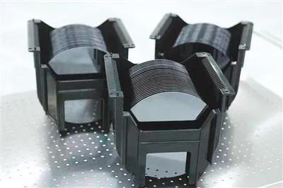
Its 8-inch semiconductor silicon polished wafer products.
这是8英寸半导体硅抛光晶圆产品。
Within a few months of its founding, the company achieved volume production of 14 inches to 19 inches. In May 2020, a high quality silicon single crystal with a diameter of 22 inches was successfully grown.
在成立后的几个月里,公司实现了14英寸到19英寸的量产。2020年5月,成功生长出直径为22英寸的高品质硅单晶。
The company's high level of product yield and quality have been recognized by foreign customers, and become a partner of competitors. The company's international market share continues to increase, successfully entered the international advanced semiconductor material industry chain system, and formed a global advantage in related segments.
公司高水平的产品良率和质量得到了国外客户的认可,并成为竞争对手的合作伙伴。公司国际市场占有率持续提升,成功进入国际先进半导体材料产业链体系,并在相关细分领域形成全球优势。
The successful development of low-defect growth technology of 8-inch crystal (i.e., wafer substrate) chip without magnetic field assistance has laid a good foundation for the development and mass production of the next 12-inch low-defect crystal chip. Many of the company's technologies are at the international advanced level.
成功开发出无需磁场辅助的8英寸晶体(即晶圆基材)芯片低缺陷生长技术,为下一阶段12英寸低缺陷晶体芯片的研发和量产奠定了良好的基础。公司多项技术处于国际先进水平。
The lithography process requires more than 100 electronic grade high-purity industrial gases to cooperate with each other, each of which is indispensable.
光刻工艺需要100多种电子级高纯工业气体相互配合,每一种都是不可或缺的。
In 2018, Hunan Kemet Gas, which purifies food-grade carbon dioxide from industrial waste gas, has become an important supplier to many international food and beverage companies. In the same year, the company made the decision to climb the new peak of electronic special gas, invested 230 million yuan, and built a new factory in Yueyang, Hunan Province, with a strong R & D team.
2018年,从工业废气中净化食品级二氧化碳的湖南凯美特气体已成为许多国际食品和饮料公司的重要供应商。同年,公司做出了勇于攀登电子特种气新高峰的决定,投资2.3亿元,在湖南岳阳新建工厂,拥有强大的研发团队。

After two years of hard technical research, the series of products will be launched in 2020. The technical team continuously sends the sample data to the major international factories, and carries out multiple certification procedures in parallel and in parallel, so as to obtain the admission ticket as soon as possible.
经过两年艰苦的技术攻关,系列产品于2020年推出。技术团队不间断地将样品数据发送到各大国际工厂,并行、并行地进行多个认证程序,争取时间尽快获得准考证。
25 sets of electronic special gas and mixture production and processing equipment have been built, extending to a full range of electronic special gas fields, forming a professional electronic special gas and mixture research and development and production and processing base with greater influence in the industry. The company will contribute to expanding market supply.
建成电子特种气和混合气生产加工设备25套,延伸到全系列电子特种气田,形成了行业内具有较大影响力的专业电子特种气和混合气研发和生产加工基地。该公司将为扩大市场供应作出贡献。
The import and export control measures of the United States will not bring any benefits, but will only promote the progress and rise of China's technology, causing many American companies to suffer certain economic losses, while seriously hurting the European semiconductor industry. The ASML CEO said that if this behavior in the United States is not stopped, European chips could disappear from the Chinese market within 15 years. The revised U.S. rules are aimed not at China but at Europe, Taiwan, South Korea and Japan, preventing other foreign chip and semiconductor equipment companies from competing with U.S. companies in the Chinese market.
美国的进出口管制措施不会带来任何好处,只会促进中国技术的进步和崛起,使许多美国企业遭受一定的经济损失,同时严重伤害欧洲半导体产业。ASML首席执行官表示,如果不停止美国的这种行为,欧洲芯片可能会在15年内从中国市场消失。美国修订后的规则并非针对中国,而是针对欧洲、台湾地区、韩国和日本,阻止其他外国芯片和半导体设备企业与美国企业争夺中国市场。
For mainland China, only by giving up illusions, focusing on solving problems, building its own core technology, strengthening national strategic scientific and technological manpower, and building an industrial ecology of its own core technology can it have a bright future.
对于中国大陆来说,只有放弃幻想,集中精力解决问题,建设自己的核心技术,加强国家战略科技人力,构建自己核心技术的产业生态,才会有光明的未来。
In 2002, the lithography machine was officially included in the "863 major scientific and technological research plan". Subsequently, under the leadership of the Ministry of Science and Technology and the Shanghai Municipal Government, a number of domestic technology companies jointly established Shanghai Microelectronics to undertake key research tasks. Among them, the focus of research and development is 100nm step scan projection lithography machine.
2002年,光刻机正式列入“863重大科技攻关计划”。随后,在科技部和上海市政府的领导下,多家国内科技企业联合成立了上海微电子,承担攻关攻关任务。其中,重点研发的是100nm步进扫描投影光刻机。
Today, Shanghai Microelectronics has become the most advanced lithography equipment manufacturer in China, with 80% of the domestic market share of packaged lithography products and 40% of the global market share. In addition, its LED/MEMS/ power device lithography machine performance indicators are leading, and its LED lithography machine market share is the largest. However, in the field of front-end lithography machines for chip manufacturing, the most advanced equipment that Shanghai Microelectronics can currently mass produce is only at the 90nm process node. Although it said that it will launch a 28-nanometer process lithograph machine in 2021, it is far from the 5-nanometer process equipment of the Dutch company ASML.
如今,上海微电子已成为国内最先进的光刻设备制造商,封装光刻产品的国内市场占有率为80%,全球市场占有率为40%。此外,其LED/MEMS/功率器件光刻机性能指标领先,其LED光刻机市场份额最大。但在用于芯片制造的前端光刻机领域,上海微电子目前能够量产的最先进设备仅在90nm工艺节点。虽然表示将在2021年推出28纳米制程光刻机,但与荷兰阿斯麦公司(ASML)的5纳米以下制程设备相差甚远。
By 1965, the first batch of integrated circuits were born in Beijing, Shijiazhuang, Shanghai and other places. This marked the beginning of the application of lithography technology in chip manufacturing.
1965年,第一批集成电路在北京、石家庄、上海等地诞生。这标志着光刻技术在芯片制造中的应用的开始。
In 1980, Tsinghua University developed a distributed projection lithography machine with an accuracy of 3 microns. In 1981, the Institute of Semiconductors of the Chinese Academy of Sciences developed the JK-1 semi-automatic proximity lithography machine. In 1982, the Chinese Academy of Sciences 109 plant developed ka-75-1 lithography machine.
1980年,清华大学研制出精度为3微米的分布式投影光刻机。在1981年,中国科学院半导体研究所发展了JK-1半自动接近光刻机。1982年,中国科学院109厂研制了ka -75-1光刻机。
The level of equipment is not low, and even close to the international mainstream level at that time. In 1985, the step projection lithography machine developed by CEC 45 was certified by the Electronic Technology Department as being up to the level of the 4800DSW lithography machine introduced by GCA in 1978.
装备水平不低,甚至接近当时的国际主流水平。1985年,CEC 45研制的分步投影光刻机被电子技术部鉴定为达到了GCA公司1978年推出的4800DSW光刻机的水平。
However, affected by this, at the beginning of the market, it conquered technology and manufacturing equipment, and it has a representative of core strength. If you look at the early development of domestic lithography machines, you can also find that the foundation was laid in the 1950s, and in the 1960s and 1970s, it took a step forward. In the early 1980s, it was second only to the United States and even ahead of Japan and Taiwan.
但受此影响,在市场化刚起步的时候就征服了技术和制造设备,更具有核心实力的代表。如果梳理一下国内光刻机的早期发展,也可以发现,50年代奠定了基础,到了60、70年代,又向前迈进了一步。在20世纪80年代初,它仅次于美国,甚至领先于日本和台湾地区。
In general, for more than two decades, the older generation of revolutionaries and builders dedicated their youth to creating a special glory for China's semiconductor industry: self-sufficiency of the whole industry chain from single crystal preparation, equipment manufacturing to integrated circuit manufacturing. The strength of self-sufficiency has gradually reached its peak, basically not dependent on foreign imports.
总的来说,二十多年来,老一辈的革命者和建设者奉献了他们的青春,为中国半导体产业创造了一个特殊的荣耀:从单晶制备、设备制造到集成电路制造的全产业链自给自足。自给自足的实力已逐渐达到顶峰,基本不依赖国外进口。
In 1985 and 1994, the 45 Research Institute of China Electronics Group developed G-line 1.5 micron and 0.8 micron step projection lithography machines respectively. In 1991, the Institute of Optoelectronics of the Chinese Academy of Sciences developed a synchrotron radiation X-ray engraving machine with a resolution of 1 micron.
1985年和1994年,中国电子集团45研究所分别研制了g线1.5微米和0.8微米分步投影光刻机。1991年,中国科学院光电子研究所研制出分辨率为1微米的同步辐射x射线雕刻机等。

In addition, in the context of opening up to the outside world, the trend of "buying is better than doing" has spread rapidly in China. Therefore, local governments have purchased and introduced a large number of foreign semiconductor equipment and production lines. A large number of enterprises have given up the policy of independence, self-reliance, blind acquisition, blind opening up, and embarked on the "trade, industry, technology" oriented development route.
此外,在对外开放的背景下,“买不如做”的趋势在中国迅速蔓延。因此,地方政府购买并引进了大量的国外半导体设备和生产线。大量企业放弃了独立自主、自力更生的政策,盲目收购、盲目开放,走上了“贸、工、技”为导向的发展路线。
Since then, due to the lack of support and top-level design, there has been a disconnect between domestic IC research, education and industry. In terms of scientific research, China follows the technical standards and systems formulated abroad. In terms of education, majors related to finance and trade became popular, while software engineers became less popular.
此后,由于缺乏支持和顶层设计,国内集成电路的研究、教育和产业出现了脱节。在科学研究方面,中国遵循国外制定的技术标准和技术体系。在教育方面,与金融和贸易相关的专业变得流行,而软件工程师变得不受欢迎。
In the semiconductor industry, some semiconductor companies are keen to assemble for foreign companies in exchange for the economic benefits of a large number of cheap labor. The few firms that still stick to their own path are squeezed by comprador and foreign capital. As a result, since 1987, China's original independent semiconductor research and industrial system has collapsed.
在半导体行业,部分半导体企业热衷于为外国企业组装,以换取大量廉价劳动力的经济利益。极少数仍然坚持自主路线的公司只能在买办和外国资本的挤压下生存。因此,自1987年以来,中国原有的独立半导体研究和工业体系已经崩溃。
In the entire 1990s, without the support of the market, funds and talents, domestic lithography machines did not achieve greater achievements, and the gap with the international level is getting larger and larger.
在整个90年代,没有市场、资金和人才的支持,国产光刻机并没有取得更大的成就,与国际水平的差距越来越大。
In addition, changes in the international political environment have brought enormous challenges. As early as under the framework of the "Paris Coordination Association", the West has been implementing high-tech embargoes on socialist countries, including restricting the export of lithography machines. With the end of the Cold War and the collapse of Batumi, China became a prime target.
此外,国际政治环境的变化也带来了巨大的挑战。早在“巴黎协调协会”框架下,西方就一直对社会主义国家实施高科技禁运,包括限制光刻机出口。随着冷战的结束和“巴统”的解体,中国成为主要目标。
In July 1996, under the leadership of the United States, 33 Western countries signed the Wassenaar Agreement on the Control of Exports of Conventional Arms and Dual-Use Items and Technologies. Batumi used to have only 17 members, while the Wassenaar Agreement now has 42, including Russia.
1996年7月,在美国的领导下,33个西方国家签署了《关于控制常规武器和两用品及技术出口的瓦森纳协定》。“巴统”过去只有17个成员国,而“瓦森纳尔协定”现在有包括俄罗斯在内的42个成员国。
Under this framework, Western countries generally follow the "N-2" principle to approve the export of semiconductor technology and lithography machines, which are always at least two generations behind the most advanced technology. If there is a proper delay in the approval process, basically China's existing equipment technology will be intentionally three generations or more behind (just second best, highest priced). Needless to say, the export of lithography machines even have more reservations, such as prohibiting the production of domestic independent chips, and prohibiting the production of chips for military scientific research and national defense. In addition, the Wassenaar Agreement also restricts the access of Chinese engineers to the core departments of well-known semiconductor companies in Europe and the United States to prevent technology leakage.
在这一框架下,西方国家一般遵循“N - 2”原则批准出口半导体技术和光刻机,这些技术总是落后于最先进的技术至少两代。如果在审批过程中有适当的延迟,基本上中国现有的设备技术将故意落后三代或更多(只是第二好,价格最高)。不用说,出口的光刻机甚至有更多的保留,比如禁止为国产自主芯片代工,禁止为军事科研和国防生产芯片。此外,《瓦森纳协议》还限制中国工程师进入欧美知名半导体公司的核心部门,防止技术泄露。
It is also worth noting that although the Wassenaar Agreement allows member states to exercise controls on their technology exports on a voluntary basis, in practice member states are influenced by the United States on important technology export decisions. For example, the United States has intervened to block the export of lithography machines and radar systems to China.
同样值得注意的是,虽然《瓦森纳协定》允许成员国在自愿的基础上对其技术出口实施控制,但实际成员国在重要的技术出口决策上都受到美国的影响。例如,美国曾干预阻止向中国出口光刻机和雷达系统。
In the case of increasingly limited external development space, in order to find a way out, China has proposed "market for technology" and significantly reduce tariffs. However, this has dealt a serious blow to the domestic integrated circuit industry, including lithography machines. Since then, the domestic lithography machine market has gradually been dominated by European, American and Japanese companies.
在外部发展空间日益受限的情况下,为了寻找出路,中国曾提出“以市场换技术”,大幅降低关税。然而,这对包括光刻机在内的国内集成电路产业造成了严重打击。此后,国内光刻机市场逐渐被欧美和日本公司所主导。
In 1999, when NATO invaded Kosovo, U.S. electronic information warfare paralyzed nearly all of Yugoslavia's Internet communications systems. This shocked the Chinese government. At that time, the Ministry of Information Industry and the Ministry of Science and Technology held several emergency meetings to discuss how to respond to such a war.
1999年,当北约入侵科索沃时,美国的电子信息战几乎瘫痪了南斯拉夫所有的网络通信系统。这震惊了中国政府。当时,信息产业部和科技部召开了几次紧急会议,讨论如何应对这样一场战争。
What threats will national information security face in the event of war with the United States?
当与美国开战时,国家信息安全将面临哪些威胁?
Based on the consideration of national information security and industrial development, in June 2000, The State Council issued Several Policies on Encouraging the development of the Software Industry and integrated Circuit Industry, that is, Document 18. Stimulated by policy subsidies and a huge market, China's entire semiconductor industry has experienced a boom in overseas returnees' entrepreneurship and independent development.
基于国家信息安全和产业发展的考虑,2000年6月,国务院发布了《关于鼓励软件产业和集成电路产业发展的若干政策》,即18号文。在政策补贴和巨大市场的刺激下,中国整个半导体产业经历了海归创业和自主发展的热潮。
In 2002, the lithography machine was included in the "863 major scientific and technological research plan". Among them, Shanghai Microelectronics has been the main undertaker of the research project, and the original distributed projection lithography R & D team of CLP 45 Branch moved to Shanghai to participate in "assistance". Since then, domestic lithography enterprises have awakened again.
2002年,光刻机被列入“863重大科技攻关计划”。其中,上海微电子一直是研究项目的主要承担者,中电45分公司原有的分布式投影光刻机研发团队搬到上海参与“协助”。此后,国内光刻机企业再次觉醒。
Unfortunately, at that time, the requirements for technology, precision and speed of lithography machines were already high. It has gradually become the product of state-of-the-art technologies in mathematics, optics, fluid mechanics, polymer physics and chemistry, surface physics and chemistry, precision instrumentation, machinery, automation, as well as software and image recognition. In addition, temperature, humidity, lighting, etc., will affect the success or failure of the final development. Almost everything was started from scratch, with many restrictions imposed by developed countries.
不幸的是,在那个时候,光刻机对技术、精度和速度的要求已经很高了。它已逐渐成为集数学、光学、流体力学、高分子物理与化学、表面物理与化学、精密仪器、机械、自动化以及软件和图像识别领域顶尖技术的产物。另外,温度、湿度、光照等都会影响到最终显影的成败。几乎所有的事情都是从零开始的,发达国家施加了许多限制。
Therefore, in 2002, China once again embarked on the first step on the difficult road of developing domestic lithography machines. In the process of developing 100nm front-end lithography machine, some personnel were transferred to develop package lithography machine.
于是,中国在2002年又一次踏上了发展国产光刻机的艰难道路的第一步。在开发100nm前端光刻机的过程中,调来部分人员开发封装光刻机。
At the beginning of the establishment of Shanghai Micro Electronics, the international lithography machine technology has made a major breakthrough. Prior to this, the photolithographic light source had remained at 193nm for as long as 20 years without progress. Scientists and industry from around the world have been discussing solutions. Finally, in 2002, TSMC's submersible 193nm solution was successful. Since then, ASML has seized the opportunity to work with TSMC to develop a prototype within a year, followed by the introduction of the immersion lithography machine XT:1700i. The device is 30% higher than the previous state-of-the-art dry lithography machine and can be used for 45nm mass production, accelerating the dominance of ASML.
上海微电子成立之初,国际光刻机技术取得了重大突破。在此之前,光刻光源一直停留在193nm,长达20年没有进步。来自世界各地的科学家和工业界一直在讨论解决方案。最终,在2002年,台积电提出的浸没式193nm解决方案获得成功。此后,ASML抓住了与台积电合作的机会,在一年内开发出原型机,随后推出了浸入式光刻机XT:1700i。该设备比之前最先进的干式光刻机提高30%,可用于45nm量产,加速了ASML的主导地位。
According to the official website of Shanghai Microelectronics, as of March 2020, the company has more than 3,200 patents and patent applications, and has excellent performance in the technical fields of lithography, laser, detection and so on.
据上海微电子官网显示,截至2020年3月,公司拥有专利及专利申请3200多项,在光刻、激光、检测等技术领域表现优异。
At the same time, China has just launched the 193nm ArF lithography machine project, which is more than 20 years behind the international level. Therefore, Shanghai Microelectronics began to catch up, and in 2007 announced a breakthrough in 365nm light wavelength DUV(Deep ultraviolet) lithography technology, developed a 90nm process distributed projection lithography machine.
与此同时,中国刚刚启动了193nm ArF光刻机项目,与国际水平相差20多年。于是,上海微电子开始奋起直追,并于2007年宣布突破365nm光波长的DUV(深紫外)光刻技术,研制出90nm工艺的分布式投影光刻机。
Foreign countries imposed a tacit embargo on Shanghai Microelectronics. This resulted in the prototype becoming a display that could not be put into commercial production. Therefore, in 2008, the state set up the "Very large scale integrated circuit manufacturing equipment and complete process Special" (Special 02), focusing on the development of high-end assembly technology, as well as materials, processes and other industrial supporting capabilities.
外国对上海微电子公司实行了默认的禁运。这导致原型机成为一个显示器,无法投入商业生产。因此,2008年,国家设立了“超大规模集成电路制造装备及成套工艺专项”(专项02),重点发展高端组装技术,以及材料、工艺等产业配套能力。
Since then, in addition to the whole machine manufacturing, the state has also supported the research and development of a number of supporting enterprises such as Changchun Institute of Optoelectronics, Shanghai Institute of Optoelectronics, and National Institute of Science and Technology Precision Exposure optical system. Kieer is responsible for the breakthrough immersion system for DUV lithography machines. With continuous investment, the lithography machine industry chain has made a breakthrough. In 2016, the first NA=0.75 projection lithography objective system developed by Goke Precision for high-end IC manufacturing in China, and the first 90nm node ArF projection lithography exposure optical system developed by King Optics have been delivered.
此后,除了整机制造外,国家还扶持了长春光电研究所、上海光电研究所、国家科技精密研究院曝光光学系统等一批配套企业的研发。奇尔机电负责突破DUV光刻机的液浸系统。随着不断的投入,光刻机产业链取得了突破。2016年,国科精密研发的国内第一台用于高端IC制造的NA=0.75投影光刻机物镜系统,以及国王光学研发的第一台90nm节点ArF投影光刻机曝光光学系统已经交付。
In the same year, Shanghai Microelectronics SSX600 series three step scan projection lithography machines realized mass production, of which SSA600/20 lithography machine resolution reached 90nm. However, this also means that it took Shanghai Microelectronics nine years to achieve the mass production of 90nm lithography machines.
同年,上海微电子SSX600系列三台步进扫描投影光刻机实现量产,其中SSA600/20光刻机分辨率达到90nm。然而,这也意味着上海微电子用了9年时间才实现了90nm光刻机的量产。
The 90nm process optical engraving machine is generally used for the production of non-core chips such as power management chips and mcu, and cannot meet the needs of products such as smart phone processors.
90nm制程光刻机一般用于电源管理芯片、mcu等非核心芯片的生产,无法满足智能手机处理器等产品的需求。
However, although the domestic lithography machine has not yet come out of the dilemma, it has seen the light in the details. In 2016, Huashuo Crystal successfully developed two sets of double bench prototypes, and passed the 02 special acceptance. Since then, Huashuo Crystal has broken the monopoly of ASML and become the second company in the world to master the technology.
然而,国产光刻机虽然还没有走出困境,但在细节上已经看到了曙光。2016年,华烁晶科成功研制出两套双工作台样机,并通过02专项验收。此后,华烁晶科打破了ASML的垄断,成为全球第二家掌握该技术的公司。
In the complex industry chain of lithography machines, it can be divided into two parts. First, the core components of the lithography machine, including light source, lens, double working stage, immersion solution, exposure optics and other key subsystems; The other is the lithographic support system. Equipment includes photoresist, photomask, adhesive development, lithographic gas and defect detection.
在光刻机复杂的产业链中,可以分为两个部分。一是光刻机的核心部件,包括光源、镜头、双工作级、浸没液、曝光光学等关键子系统;另一个是光刻支撑系统。设备包括光刻胶、光掩膜、胶粘剂显影、光刻气体和缺陷检测等。
On June 21, 2017, the "Key technologies of extreme ultraviolet lithography" led by Changchun Institute of Optics, Fine Mechanics and Physics of the Chinese Academy of Sciences (now Beijing Guowang Optics) passed acceptance. In November 2018, the "super resolution lithography equipment" developed by the Chinese Academy of Sciences passed acceptance. Its lithographic resolution is as high as 22nm, and combined with double exposure technology, it can also be used to manufacture 10nm class chips in the future. In 2019, Tsinghua University and Huashuo Precision two-stage system completed the development and trial production base construction.
2017年6月21日,中科院长春光学精密机械与物理研究所(现北京国望光学)牵头的“极紫外光刻关键技术”通过验收。2018年11月,中科院研制的“超分辨率光刻设备”通过验收。其光刻分辨率高达22nm,结合双曝光技术,未来还可用于制造10nm级别的芯片。2019年,清华大学与华烁精密双级系统完成研制和试产基地建设。
The success of the two-stage exposure system and the key system has become the starting point of the domestic lithography industry chain. At present, the immersion system jointly developed by the State Key Laboratory of Fluid Power and Electromechanical Systems of Zhejiang University and Qier Electromechanical ranks third in the world.
曝光系统与关键系统双阶段的成功,成为国内光刻机产业链的起点。目前,由浙江大学流体动力与机电系统国家重点实验室与祁尔机电共同研发的浸入式系统位居世界第三。
The excimer laser light source system of the Institute of Optoelectronics of the Chinese Academy of Sciences is in charge of industrial transformation by Beijing Keyi Hongyuan. The research results of 40W 4kHz ArF light source are presented. This achievement ranks third in the world.
中国科学院光电子研究所的准分子激光光源系统由北京科益宏远负责产业转型。给出了40W 4kHz ArF光源的研究成果。这一成就位居世界第三。
Specifically, Shanghai Microelectronics will be responsible for the design and overall integration of the 28-nanometer lithography machine. Keyi Hongyuan provides the light source system, Guowang Optics provides the objective lens system, and Guoke Precision provides the exposure optical system. Huashuo Crystal Co., Ltd. provides dual workbenches, and Keer Electric Co., Ltd. provides immersion systems.
具体来说,上海微电子将负责28纳米光刻机的设计和整体集成。科益宏远提供光源系统,国旺光学提供物镜系统,国科精密提供曝光光学系统。华烁晶科提供双工作台,奇尔机电提供浸入式系统。
Once the domestic lithography machine breaks through the technology below 28nm, China will have a great market potential trend. In terms of equipment categories, lithography machines are divided into front lithography machines and back lithography machines. The front lithography machine is used for chip manufacturing, and the back lithography machine is mainly used for chip packaging. Shanghai Microelectronics is the leading player in the field of back-end lithography.
一旦国产光刻机突破28nm以下技术,中国将有很大的市场潜力趋势。在设备类别上,光刻机分为正面光刻机和背面光刻机。正面光刻机用于芯片制造,背面光刻机主要用于芯片封装。上海微电子是后端光刻机领域的主导者。
In terms of process technology, the lithography machine can be divided into maskless lithography machine and mask lithography machine. The former has relatively low technical barriers and is generally used in specific chip fields such as high-resolution masks and integrated circuit prototype verification chips. Mask lithography machines with high technical barriers are mostly used in the front end of advanced manufacturing processes.
从工艺技术上讲,光刻机可分为无掩模光刻机和掩模光刻机。前者技术壁垒相对较低,一般用于高分辨率掩模、集成电路原型验证芯片等特定芯片领域。技术壁垒较高的掩模光刻机多用于先进制造工艺的前端工序。
If further subdivided, the maskless lithography machine can be divided into electron beam direct writing lithography machine, ion beam direct writing lithography machine, laser direct writing lithography machine. Mask lithography machines can be divided into contact/proximity lithography machines and projection lithography machines. In addition, the mask lithography machine can also be divided according to the production of the lithography light source.
如果再细分,无掩模光刻机可分为电子束直写光刻机、离子束直写光刻机、激光直写光刻机。掩模光刻机可分为接触式/接近式光刻机和投影式光刻机。另外,掩模光刻机还可以根据光刻光源的产生进行划分。
At present, the 193nm wavelength ArF(argon fluoride) immersion lithography machine being developed by Shanghai Microelectronics belongs to the fourth generation lithography machine, which can be used to produce 45-22nm process chips. The fifth-generation EUV lithography machine uses a 13.5nm wavelength light source and is an indispensable tool to break through the 7nm chip process node.
目前上海微电子正在研发的193nm波长ArF(氟化氩)浸没式光刻机属于第四代光刻机,可用于生产45-22nm制程芯片。第五代EUV光刻机采用13.5nm波长光源,是突破7nm芯片制程节点不可或缺的工具。
As the fourth generation light source in the history of mask lithography, the 193nm optical wavelength ArF is already the world's leading level of DUV lithography. Therefore, if Shanghai Microelectronics successfully designs and integrates the ArF immersion lithography machine with a wavelength of 193nm, it will mean that it is close to or catch up with ASML in the field of DUV lithography machines.
作为掩模光刻机历史上的第四代光源,193nm光波长ArF已经是世界领先水平的DUV光刻机。因此,如果上海微电子成功设计并集成了波长为193nm的ArF浸没式光刻机,将意味着其在DUV光刻机领域接近或赶超ASML。
EUV lithography is not required. The case often used to support this view is that SMIC's N+1 and N+2 generation processes do not use EUV processes, while TSMC only started to introduce EUV lithography machines in the third generation 7nm process.
不需要EUV光刻机。经常被用来支持这一观点的案例是中芯国际的N+1和N+2代工艺不会使用EUV工艺,而台积电在第三代7nm工艺中才开始引入EUV光刻机。
Shanghai Microelectronics has long had only a few hundred R&D staff, reaching 1,150 in early 2019. Under the obstruction of the United States, independent research and development of lithography technology has become significant. China needs to increase its technology and patent accumulation. In the international competition, the innovation and development of lithography machine technology is a multi-dimensional contest.
上海微电子长期以来只有几百名研发人员,2019年初达到1150人。在美国百般阻挠下,自主研发光刻技术变得意义重大。中国需要增加技术和专利积累。在国际竞争中,光刻机技术的创新与发展是一场多维度的较量。
Entering the new century, the entire Chinese semiconductor industry suddenly realized. Nine years later, Shanghai Microelectronics breakthrough 90nm lithography machine technology, nine years later to achieve mass production; Its 193nm optical wavelength ArF immersion lithography machine has taken nearly 20 years to achieve a breakthrough.
进入新世纪,整个中国半导体产业迎来曙光。9年后,上海微电子突破90nm光刻机技术,9年后实现量产;其193nm光波长ArF浸没式光刻机历经近20年才取得突破。
In the field of lithography machines, we need a strong strategic investment from the active and promising Chinese government, and we need the collaborative development of the government, scientific research and enterprises, because this is a country
在光刻机领域,需要积极有为的中国政府的大力战略投入,需要政府、科研、企业的协同发展,因为这是一个国家
Over the past 26 years, more than 400 enterprises and more than 300,000 scientists, engineers and technicians have participated in the construction of the BDS, which has conquered more than 160 key core technologies such as inter-satellite links and high-precision atomic clocks, and the localization rate of core components has reached 100 percent. Beidou navigation technology and ground enhancement technology integration, 5G, Internet of things, mobile Internet, cloud computing, edge computing, artificial intelligence, mechanism model and other new technology cluster, Beidou system has been applied to smart city, wearable devices, intelligent manufacturing, Internet of things, automatic driving, public infrastructure automation monitoring, smart agriculture, power grid security maintenance and other fields.
26年来,全国400多家企业、30多万名科学家、工程师和技术人员参与了北斗系统的建设,先后攻克了星间链路、高精度原子钟等160多项关键核心技术,核心部件国产化率达到100%。北斗导航技术与地面增强技术融合,5G、物联网、移动互联网、云计算、边缘计算、人工智能、机制模型等新技术集群,北斗系统已应用于智慧城市、可穿戴设备、智能制造、物联网、自动驾驶、公共基础设施自动化监控、智慧农业、电网安全维护等领域。
These 300,000 or so scientists, engineers and technicians can help domestic lithography machines break through the technology below 28nm and complete the goal of manufacturing in China by 2025.
这30万左右的科学家、工程师和技术人员可以帮助国产光刻机突破28nm以下的技术,并在2025年之前完成中国制造的目标。
Nowadays, the state's support for independent innovation is unprecedented, and Chinese people must cherish this special era. The logic behind the lithography machine industry is that it can manufacture mobile phones, computers, televisions, missiles, space shuttles and other equipment chips, involving the national economy and people's livelihood, but also involving the development of science and technology, military, and social economy. In a people's country, this cause is bound to receive strong support. At present, the funds are in place, the industrial chain is gathered around the future lithography giants in mainland China, and all links of the industrial chain such as double tables, optics, light sources, objective lenses, and immersion systems are mobilized. A temporarily backward but basically self-sufficient industrial chain is slowly growing in China.
如今,国家对自主创新的支持是前所未有的,中国人必须珍惜这个特殊的时代。光刻机产业背后的逻辑是,它可以制造手机、电脑、电视、导弹、航天飞机等设备芯片,涉及国计民生,也涉及科技、军事、社会经济的发展。在一个人民的国家里,这项事业必然会得到大力支持。目前,资金到位,产业链聚集在中国大陆未来的光刻机巨头周围,双工作台、光学、光源、物镜、浸入系统等产业链的各个环节都被调动起来。一条暂时落后但基本可以自给自足的产业链正在中国慢慢成长。
Shanghai Microelectronics has said that a new generation of domestic lithography machines is expected to be mass-produced in 2021, and a domestic 28nm chip production line is expected to be built in 1-2 years.
上海微电子已经表示,新一代国产光刻机预计将于2021年量产,国产28nm芯片生产线预计将在1-2年内建成。
As of June 25, 2021, Huawei has completed the assembly of a fully autonomous and controllable 28nm chip production line. As long as Shanghai Microelectronics delivers the 28nm lithography machine on time in the second half of 2021, Huawei can achieve the mass production of 28nm chips. Qualcomm has not been helpful, and while it is approved to supply Huawei, they are outdated chips. We're not laying people off. In the future, Huawei will not only design high-end chips, but also produce high-end chips.
截至2021年6月25日,华为完成了完全自主可控的28nm芯片生产线的组装工作。只要上海微电子在2021年下半年按时交付28nm光刻机,华为就可以实现28nm芯片的量产。高通一直没有提供帮助,虽然它被批准向华为供应,但它们都是过时的芯片。我们不会裁员。华为未来不仅会设计高端芯片,还会生产高端芯片。
Even if the U.S. government continues to take tough measures to block and isolate scientific and technological personnel on China-related issues, it is almost impossible for the United States to confront China, which has a strong endogenous resource capacity. Only by adhering to the original intention of innovation and following the laws of technology and the market can China have a bright future. Using politics as a weapon, or being used by political forces, will eventually pay a price in the market.
即使美国政府在涉华问题上继续采取强硬手段封锁和孤立科技人员,美国也几乎不可能对抗拥有极强内生资源能力的中国。只有坚持创新的初心,遵循技术和市场的规律,中国人才能拥有光明的未来。把政治当作武器,或者被政治势力利用,最终都会在市场上付出代价。
In the future, China will continue to increase investment in research and development, strengthen the construction of talent teams, focus on the pursuit of excellent quality, and consolidate technology.
未来,中国将继续加大研发投入,加强人才队伍建设,专心追求卓越品质,夯实技术。
They have overcome many production problems and filled domestic gaps, while expanding China's semiconductor industry chain and attracting more high-quality foreign investment, high-end talents and advanced technologies.
他们攻克了许多生产难题,填补了国内空白,同时扩大了中国半导体产业链,吸引了更多优质外资、高端人才和先进技术。
In addition, cyber attacks on China by the United States have increased year after year.
此外,美国对中国的网络攻击也连年增加。
Who is to blame for these not-so-smart moves?
谁该为这些不太聪明的举动负责呢?
This is part of a view on whether China can develop a fully autonomous chip manufacturing system without relying on any foreign technology.
这是对中国能否在不依赖任何外国技术的情况下发展出完全自主的芯片制造体系的部分看法。
It's another day in the sun.
这是阳光下的另一天。


